
Electron and Scanning Probe Microscopy Solutions
Explore nanoscale imaging systems from MICROSCOPY AND IMAGING designed for research, diagnostics, and advanced materials analysis across North America.

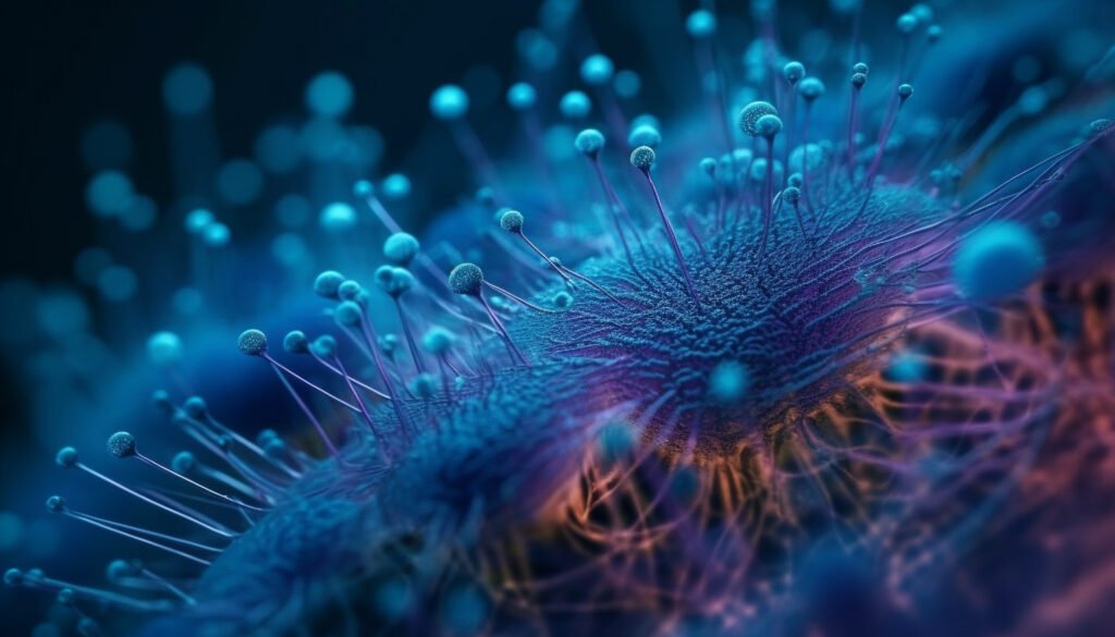
High-Resolution Imaging Beyond Optical Limits
Electron and Scanning Probe Microscopy encompasses a powerful group of imaging technologies designed to visualize materials and biological specimens at nano meter to atomic resolutions. These systems go far beyond the limits of optical microscopy, using electron beams or fine-tipped probes to examine surface structure, internal composition, and nanoscale interactions. Techniques such as Transmission Electron Microscopy (TEM), Scanning Electron Microscopy (SEM), Atomic Force Microscopy (AFM), and Scanning Tunnelling Microscopy (STM) play crucial roles in disciplines ranging from semiconductor design to structural biology.
Across North America, MICROSCOPY AND IMAGING supports businesses and institutions with integrated, high-performance electron and scanning probe microscopy solutions. As a trusted B2B technology partner, we deliver systems tailored for precision, stability, and throughput. Our team works closely with clients to provide custom configurations, seamless integrations, and long-term technical support. Through continuous product development, innovation, and rigorous quality assurance, we help organizations unlock the full potential of nanoscale imaging.
Electron and Scanning
Probe Microscopy
MICROSCOPY AND IMAGING offers a wide portfolio of Electron and Scanning Probe Microscopy (ESPM) technologies to meet the specialized needs of research, manufacturing, and advanced materials characterization.

Transmission Electron Microscopy (TEM)
- Uses transmitted electron beams to image thin sections of samples
- Achieves atomic-level resolution
Ideal for detailed cellular ultrastructure, advanced nanomaterials, and crystallography research.
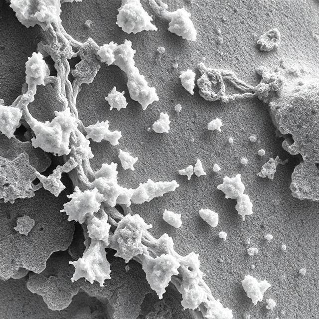
Scanning Electron Microscopy (SEM)
- Uses focused electron beams to scan sample surfaces
- Provides high-contrast, 3D-like surface imaging
- Widely used in failure analysis, surface topography, and microfabrication
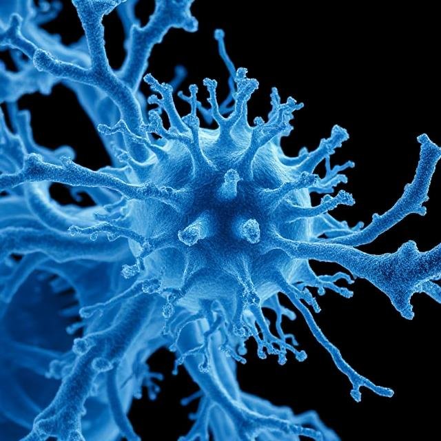
Cryo-Electron Microscopy (Cryo-EM)
- Captures biological samples in near-native states via vitrification
- Essential for macromolecular structure determination
- Eliminates the need for staining, fixing, or other sample preparation steps.
Atomic Force Microscopy (AFM)
- Uses a nanoscale mechanical probe to measure surface features
- Enables topographical mapping, force measurements, and elasticity testing
- Operates in air, vacuum, or liquid environments

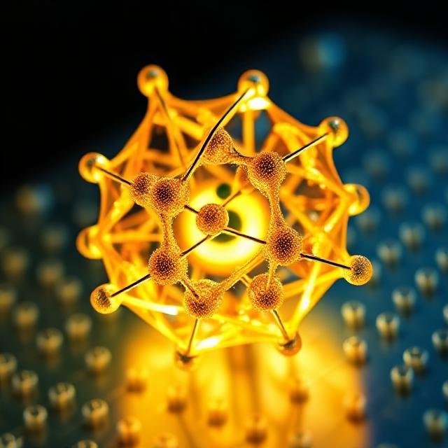
Scanning Tunnelling Microscopy (STM)
- Maps surface atoms by measuring quantum tunnelling current
- Enables atomic-level visualization of conductive materials
- Commonly used in nanotechnology and semiconductor research & development.
Each system can be customized with advanced detectors, environmental chambers, or hybrid modules to fit the demands of specific industries.
Ready to take your imaging to the next level?
Connect with us for expert guidance, customized system configurations, and comprehensive support tailored to your specific applications. Whether you are working in materials science, biotechnology, or semiconductor research, we are here to deliver the right solution for your imaging challenges.