
Unveiling Atomic Detail with High-Resolution TEM
MICROSCOPY AND IMAGING delivers advanced TEM systems for nanometer and atomic-level imaging in materials science, biology, and industrial R&D.

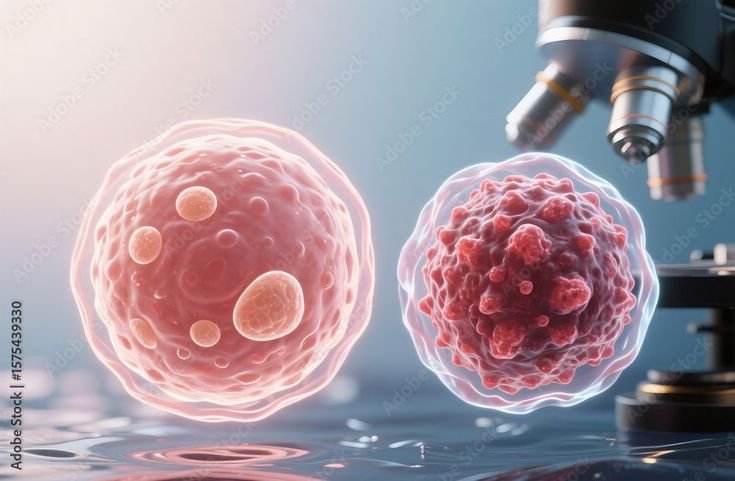
High-Resolution TEM Solutions for Advanced Research and Industry
Transmission Electron Microscopy (TEM) is a cutting-edge imaging technique that enables visualization of materials at nanometer and even atomic resolutions. Unlike light-based systems, TEM transmits a beam of electrons through ultra-thin samples, capturing detailed internal structures with unmatched clarity. It’s a core technology in nanotechnology, structural biology, and materials characterization.
TEM is widely used across North America in both research and industrial applications. MICROSCOPY AND IMAGING provides high-performance TEM systems to B2B clients seeking superior imaging accuracy, repeatability, and system integration. Our TEM solutions are designed for labs, universities, and production environments where resolution, throughput, and versatility are essential. With expertise in system configuration, support, and innovation, MICROSCOPY AND IMAGING helps organizations stay ahead with scalable solutions backed by a strict quality assurance process and customer-first service approach.
Core Components of TEM Systems
In addition to offering products and systems developed by our team and trusted partners for Transmission Electron Microscopy (TEM), we are proud to carry top-tier technologies from Global Advanced Operations Tek Inc. (GAO Tek Inc.) and Global Advanced Operations RFID Inc. (GAO RFID Inc.). These reliable, high-quality products and systems enhance our ability to deliver comprehensive technologies, integrations, and services you can trust. Where relevant, we have provided direct links to select products and systems from GAO Tek Inc. and GAO RFID Inc.
Hardware
- High-resolution electron detectors and scintillators
Flaw Detectors(Structural Testers) – essential for identifying atomic-level defects and material inconsistencies. - Vacuum chamber enclosures with precision alignment
Fiber Optic Multimeters(Fiber Networks) – enabling alignment accuracy and environmental stability within the vacuum system. - Beam control and focusing units with electromagnetic lenses
Function Generators(Electrical Testers) – used to fine-tune and stabilize electromagnetic lens fields for imaging resolution. - Cryo-holders and temperature stabilization accessories
Temperature Data Loggers(Environmental Test Instruments) – ensuring precise thermal regulation during nano-scale imaging sessions. - Stage controllers and nanometer positioning systems Motion & Position Sensors (IoT Sensors) – supporting ultra-fine movement control and sample manipulation in real time
Software
- Real-time image acquisition with adjustable contrast and magnification
- Automated alignment, focusing, and beam calibration
- Digital image processing and 3D reconstruction tools
- Elemental analysis integration via EDS (Energy Dispersive X-ray Spectroscopy)
- Data export options for integration with external databases and reporting systems
Cloud Services
- Secure backup of high-resolution image datasets
- Real-time remote access and control for multi-site teams
- Integration with lab-wide data management systems
- AI-assisted image classification and defect recognition (where supported)
Key Features and Functionalities
- Imaging resolution down to 0.1 nanometers
- Suitable for both biological and material science applications
- Internal structural analysis of cells, polymers, metals, and semiconductors
- Elemental analysis capabilities when paired with spectrometry tools
- Sample tilting, rotation, and cryogenic conditions for advanced studies
- Time-resolved imaging for dynamic material behavior studies
Integrations
MICROSCOPY AND IMAGING’s TEM systems integrate seamlessly with:
- Energy-dispersive spectroscopy (EDS) and electron energy loss spectroscopy (EELS) modules
- Digital Laboratory Information Management Systems (LIMS)
- Sample prep stations and microtome tools
- AI-based image processing workflows
- Advanced control interfaces for remote or automated operations
Compatibility
- Compatible with sample holders and prep equipment from major brands
- Modular design for integration with cryo-sample workflows
- Interfaces with Windows, Linux, and proprietary control systems
- Data export formats compatible with major analysis platforms
- Custom API support available for automation and custom scripting
Benefits
- Unmatched resolution and structural clarity
- Enables visualization of atomic and sub-cellular features
- Scalable from academic research to industrial failure analysis
- Extendable with add-on modules for spectroscopy and tomography
- Reduces rework and accelerates R&D with precise material insights
- Long-term support and upgrade paths for evolving imaging needs
Applications
- Structural analysis of metals, ceramics, and semiconductors
- Biological ultrastructure imaging (e.g., viruses, organelles)
- Defect detection and failure analysis in manufacturing
- Nanomaterial characterization and development
- Academic research and education in materials science
- Battery material and catalyst structure optimization
Industries
- Materials Science & Nanotechnology
- Biomedical & Life Sciences
- Semiconductor & Electronics Manufacturing
- Energy Storage & Battery Research
- Aerospace Engineering
- Research Universities & Government Labs
Relevant Industry Standards
ISO/IEC 17025
ASTM E766
ANSI/NCSL Z540-1
FDA 21 CFR Part 11
Health Canada Medical Device Licensing (MDL)
Case Studies
U.S. Aerospace R&D Lab, Ohio
A defense contractor collaborated with MICROSCOPY AND IMAGING to install a customized TEM solution for characterizing aerospace alloy structures at the atomic level. The system’s high-resolution imaging revealed microstructural anomalies in composite materials, leading to design improvements that extended part life by 18%.
Medical Research Center, Maryland
A leading biomedical institute integrated our cryo-TEM solution for studying virus morphology. With sub-nanometer resolution, the center advanced its vaccine research pipeline and published groundbreaking findings on viral replication in leading scientific journals.
Nanotech Lab, Alberta
MICROSCOPY AND IMAGING provided a nanotechnology lab with a field-emission TEM system to analyze nanostructured coatings. The integration of EDS allowed for elemental mapping, which helped the lab improve the performance of protective coatings used in industrial tools.
Need expert guidance on implementing Transmission Electron Microscopy in your lab or facility?
Contact with us to speak with our technical specialists. We are ready to help you design and deploy a customized, scalable TEM solution that supports your scientific, research, or manufacturing goals.